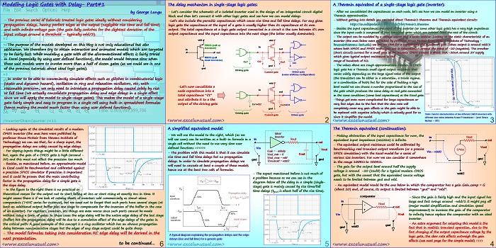
After learning how to model ideal logic gates in MS Excel 2003 it is time to attemp to create a delay based model. This first model is just a theoretical presentation about delay, how it can be explained and how it can be modeled with a minimum amount of formulas while keeping a reasonable precision. The presentation focuses on the basic CMOS inverter and it shows that for a basic single-stage logic gate the delay is mainly driven by the product between an equivalent Thevenin output impedance and the capacitance seen at the output of the gate, which obviously includes the input capacitance of the following stage and perhaps the transmission line capacitance.
↧
